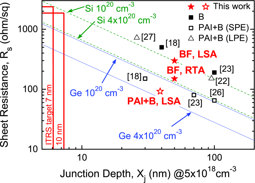
Laser Spike Annealing for Shallow Junctions in Ge CMOS
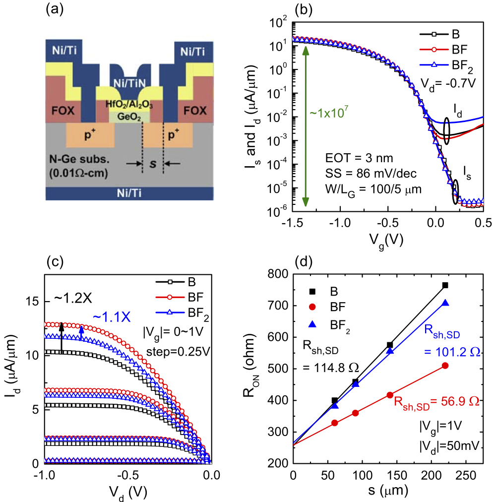
Novel BF+ implantation for high-performance Ge pMOSFETs
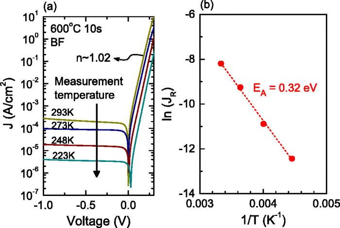
Diffusion and recrystallization of B implanted in Ge in presence of F
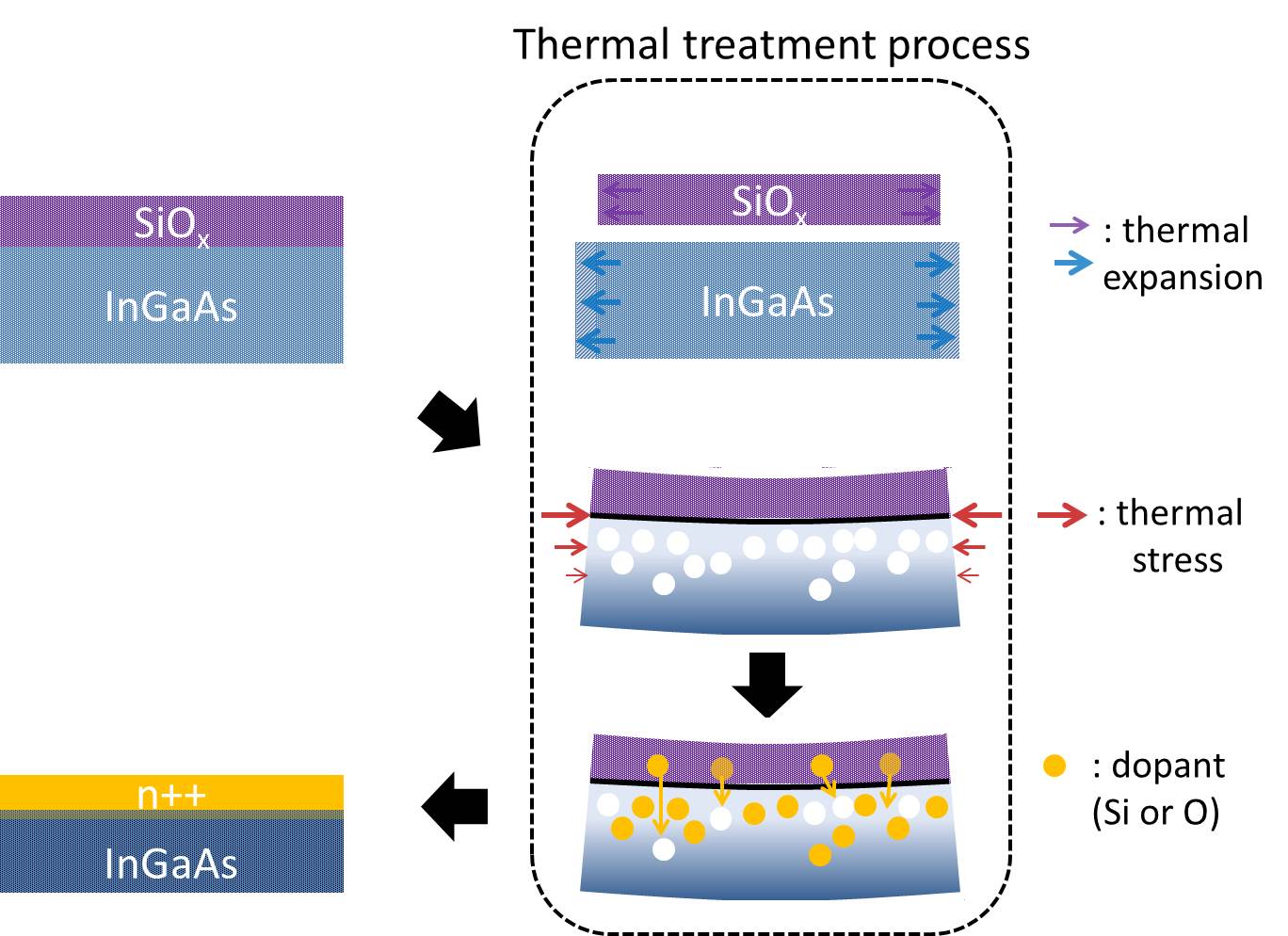
Doping enhancement of compound
semiconductors (InGaAs) via solid source dopant
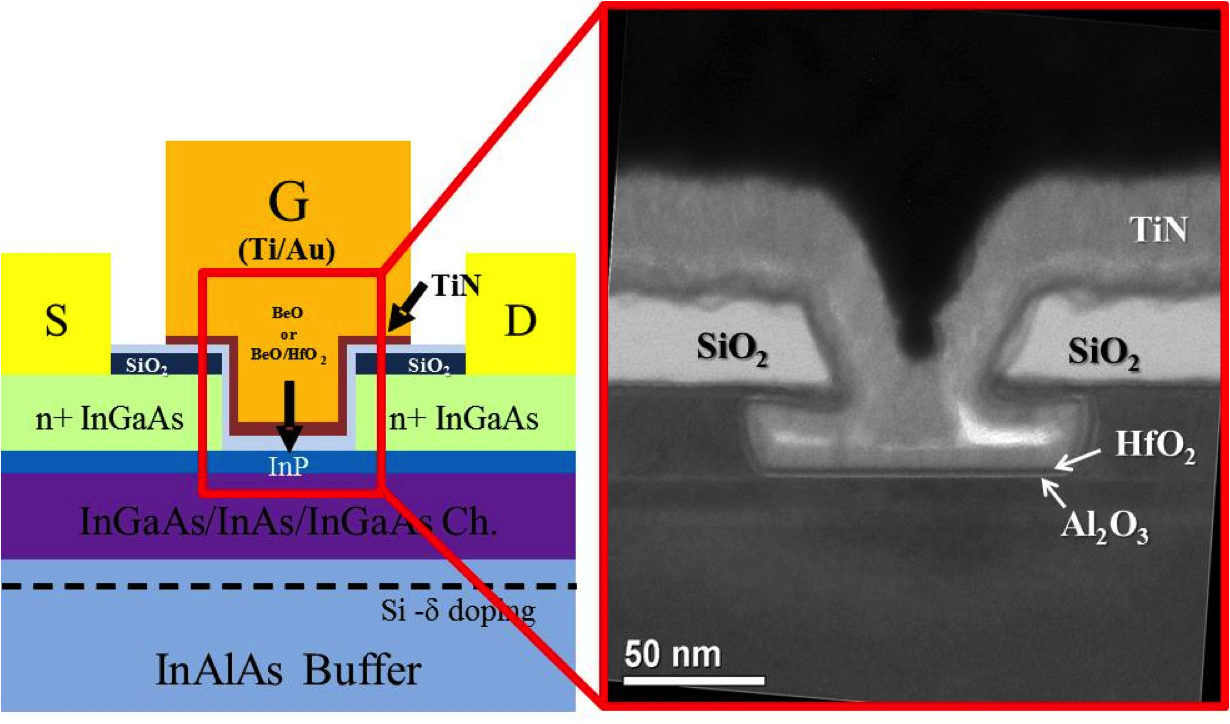
QW MOSFETs with BeO and BeO/HfO2
as gate dielectric and interfacial layer

Growth optimization of Ge1-xCx and
development of buried-channel pMOSFET
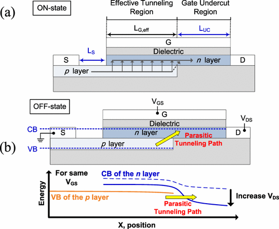
Electrostatic Control of Gate-Normal-TFETs
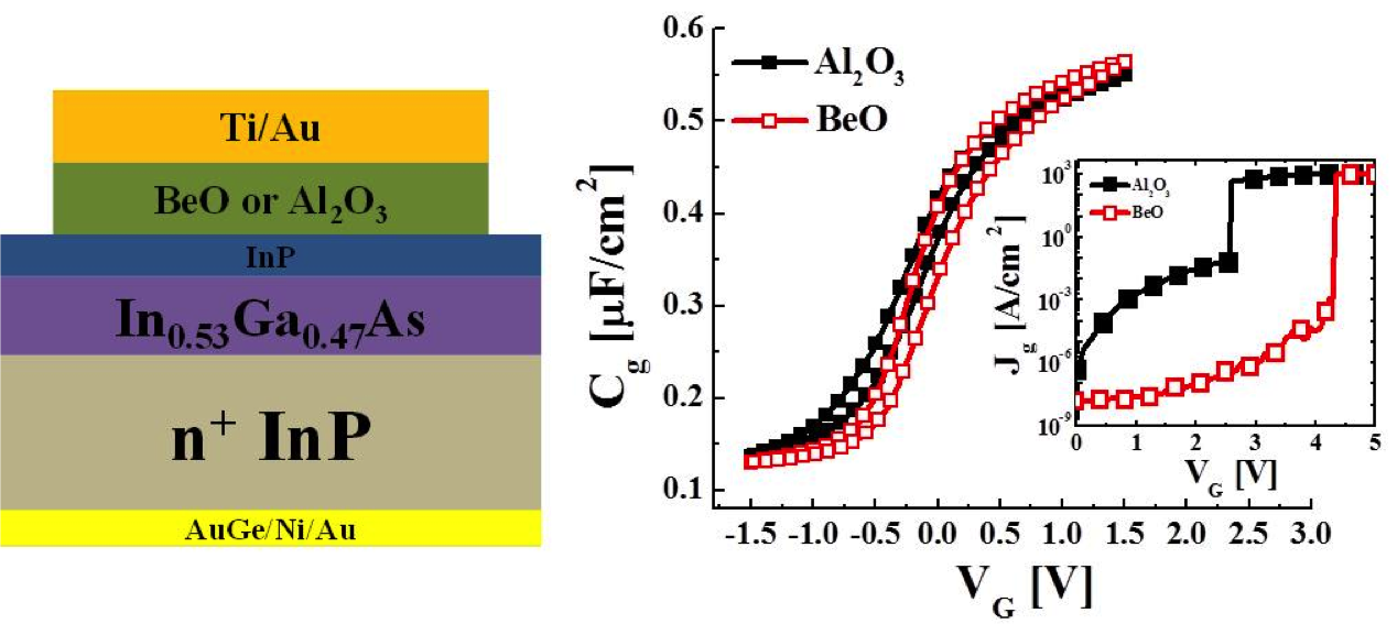
Optimization of ALD BeO as MOS gate dielectric
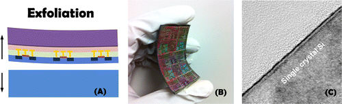
High-Performance Flexible Thin-Film
Transistors Exfoliated from Bulk Wafer
Si/Ge and III-V Electronics
Future Si CMOS scaling is reaching practical and fundamental limits. The strained-Si technology (SiGe embedded S/D etc.) is gradually approaching its limits as a performance booster in non-planar devices due to the challenges of integration. In order to reduce power while maintaining performance for future technology nodes, high mobility materials, such as Ge and III-V together with advanced device structures are being aggressively explored to increase the drive current and reduce switching times. Current research focuses on:
- Exploring heterogeneous integration of the high mobility Ge on Si substrate and the technologies to enable high performance Ge nMOS and pMOS for sub-10 nm
- Novel damage-free doping mechanisms for compound semiconductors
- Development and optimization of BeO as gate dielectric for MOS structures
Recent Publications:
- William Hsu, Feng Wen, Xiaoru Wang, Yun Wang, Andrei Dolocan, Anupam Roy, Taegon Kim, Emanuel Tutuc, and Sanjay K. Banerjee. Laser Spike Annealing for Shallow Junctions in Ge CMOS. IEEE Transactions on Electron Devices, 64(2):346--352, February 2017. [DOI | http ]
- William Hsu, Xiaoru Wang, Feng Wen, Yun Wang, Andrei Dolocan, Taegon Kim, Emanuel Tutuc, and Sanjay K. Banerjee. High Phosphorus Dopant Activation in Germanium Using Laser Spike Annealing. IEEE Electron Device Letters, 37(9):1088--1091, September 2016. [DOI | http ]
- W. Hsu, T. Kim, H. Chou, A. Rai, and S. K. Banerjee. Novel BF+ Implantation for High Performance Ge pMOSFETs. IEEE Electron Device Letters, 37(8):954-957, August 2016. [DOI ]
- William Hsu, Taegon Kim, Alfredo Benítez-Lara, Harry Chou, Andrei Dolocan, Amritesh Rai, M. Josefina Arellano-Jiménez, Marylene Palard, Miguel José-Yacamán, and Sanjay K. Banerjee. Diffusion and recrystallization of B implanted in crystalline and pre-amorphized Ge in the presence of F. Journal of Applied Physics, 120(1):015701, July 2016. [DOI | http ]
- Jaehyun Ahn, Harry Chou, Donghyi Koh, Taegon Kim, Anupam Roy, Jonghan Song, and Sanjay K. Banerjee. Nanoscale doping of compound semiconductors by solid phase dopant diffusion. Applied Physics Letters, 108(12):122107, March 2016. [DOI | http ]
- Donghyi Koh, Seung Heon Shin, Jaehyun Ahn, Sushant Sonde, Hyuk-Min Kwon, Tommaso Orzali, Dae-Hyun Kim, Tae-Woo Kim, and Sanjay K. Banerjee. Damage free Ar ion plasma surface treatment on In0.53Ga0.47As-on-silicon metal-oxide-semiconductor device. Applied Physics Letters, 107(18):183509, November 2015. [ DOI | http ]
- W. Hsu, J. Mantey, L.F. Register, and S.K. Banerjee. On the Electrostatic Control of Gate-Normal-Tunneling Field-Effect Transistors. IEEE Transactions on Electron Devices, 62(7):2292-2299, July 2015. [ DOI ]
- Yujia Zhai, L. Mathew, R. Rao, M. Palard, S. Chopra, J.G. Ekerdt, L.F. Register, and S.K. Banerjee. High-Performance Vertical Gate-All-Around Silicon Nanowire FET With High-κ/Metal Gate. IEEE Transactions on Electron Devices, 61(11):3896-3900, November 2014. [ DOI ]
- William Hsu, Jason Mantey, Cheng-Chih Hsieh, Anupam Roy, and Sanjay K. Banerjee. Thin, relaxed Si1−xGex virtual substrates on Si grown using C-doped Ge buffers. Applied Physics Letters, 105(15):152107, October 2014. [ DOI | http ]
- T.-W. Kim, D.-H. Kim, D.H. Koh, H.M. Kwon, R.H. Baek, D. Veksler, C. Huffman, K. Matthews, S. Oktyabrsky, A. Greene, Y. Ohsawa, A. Ko, H. Nakajima, M. Takahashi, T. Nishizuka, H. Ohtake, S.K. Banerjee, S.H. Shin, D.-H. Ko, C. Kang, D. Gilmer, R.J.W. Hill, W. Maszara, C. Hobbs, and P.D. Kirsch. Sub-100 nm InGaAs quantum-well (QW) tri-gate MOSFETs with Al2O3/HfO2 (EOT < 1 nm) for low-power logic applications. In Electron Devices Meeting (IEDM), 2013 IEEE International, pages 16.3.1-16.3.4, December 2013. [ DOI ]
- William Hsu, Jason Mantey, Leonard F. Register, and Sanjay K. Banerjee. Strained-Si/strained-Ge type-II staggered heterojunction gate-normal-tunneling field-effect transistor. Applied Physics Letters, 103(9):093501, August 2013. [ DOI | http ]
- J. Mantey, W. Hsu, J. James, E. U. Onyegam, S. Guchhait, and S. K. Banerjee. Ultra-smooth epitaxial Ge grown on Si(001) utilizing a thin C-doped Ge buffer layer. Applied Physics Letters, 102(19):192111, May 2013. [ DOI | http ]
- T.-W. Kim, D. Kim, D.-H. Koh, R.J.W. Hill, R.T.P. Lee, M.H. Wong, T. Cunningham, J.A. Del Alamo, S.K. Banerjee, S. Oktyabrsky, A. Greene, Y. Ohsawa, Y. Trickett, G. Nakamura, Q. Li, K.M. Lau, C. Hobbs, P.D. Kirsch, and R. Jammy. ETB-QW InAs MOSFET with scaled body for improved electrostatics. In Electron Devices Meeting (IEDM), 2012 IEEE International, pages 32.3.1-32.3.4, December 2012. [ DOI ]
- Yujia Zhai, Leo Mathew, Rajesh Rao, Dewei Xu, and Sanjay K. Banerjee. High-Performance Flexible Thin-Film Transistors Exfoliated from Bulk Wafer. Nano Lett., 12(11):5609-5615, November 2012. [ DOI | http ]
- Junghyo Nah, David C. Dillen, Kamran M. Varahramyan, Sanjay K. Banerjee, and Emanuel Tutuc. Role of Confinement on Carrier Transport in Ge–SixGe1–x Core–Shell Nanowires. Nano Lett., 12(1):108-112, January 2012. [ DOI | http ]
- Jung Hwan Yum, G. Bersuker, T. Akyol, D.A. Ferrer, Ming Lei, Keun Woo Park, T.W. Hudnall, M.C. Downer, C.W. Bielawski, E.T. Yu, J. Price, Jack C. Lee, and Sanjay K. Banerjee. Epitaxial ALD BeO: Efficient Oxygen Diffusion Barrier for EOT Scaling and Reliability Improvement. IEEE Transactions on Electron Devices, 58(12):4384-4392, December 2011. [ DOI ]